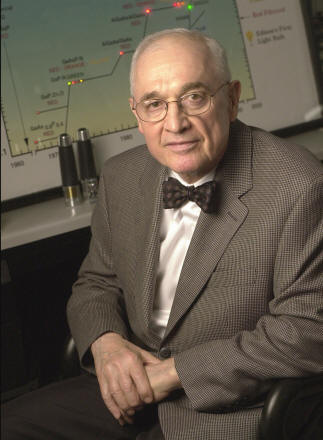
Nick Holonyak Jr.
Pioneer in semiconductors
During his career Nick Holonyak improved and developed transistors, thyristors, triacs, methods of semiconductor crystal growth, tunnel diodes, lasers, red LEDs.
 |
|
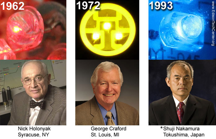
He was the first to make silicon tunnel diodes and observe phonon-assisted tunneling (1959), the first observation of inelastic tunneling and the beginning of tunneling spectroscopy. He invented (1960) closed-tube vapor phase epitaxy of III-V semiconductors, the forerunner of all present-day III-V VPE crystal growth. Besides early work (1960-62) on III-V heterojunctions, he was the first (1960) to grow GaAs1-xPx (an alloy) and to construct visible-spectrum lasers and light emitting diodes (1962), thus proving that III-V alloys are “smooth" and viable, in general, for use in optoelectronic devices. He is the inventor of the first practical LED, the red GaAs1-xPx LED, which also marks the beginning in the use of III-V alloys in semiconductor devices, including in heterojunctions and quantum well heterostructures (QWHs).
Besides demonstrating the visible-spectrum laser operation of the alloys GaAsP (1962), InGaP (1970), AlGaAsP (1970), and InGaPAs (1972), he and his student Rezek made (via LPE, 1977) the first quantum well (QW) laser diodes. Later, with Dupuis (and MOCVD AlGaAs-GaAs), he demonstrated (1978) the initial continuous 300 K operation of a QW laser, and introduced the name “quantum well laser.” He and his students introduced (1980) impurity induced intermixing (~ 600°C) of QW heterostructure (QWH) and superlattice layers, and with it the selective shift from QW lower gap to bulk-crystal higher gap (used to define waveguide and laser geometries).
In 1990 he and his students introduced the Al-based III-V native oxide into optoelectronics, including its use as a buried oxide aperture to define the current and cavity in lasers (now used in VCSELs). He is currently concerned with coupled quantum-dot/quantum well-lasers. His work has led to 500+ papers and 31 patents.

Organizations and Awards:
Holonyak is a member of NAE (1973), NAS (1984), American Academy of Arts and Sciences (Fellow, 1984), Russian Academy of Sciences (Foreign Member, 1999), American Physical Society (Fellow), Institute of Electrical and Electronics Engineers (Life Fellow), Optical Society of America (Fellow), Am. Assoc. Adv. Science (Fellow), Electrochemical Society, and Mathematical Association of America.
He has received a number of awards, including: Cordiner Award (1962, GE); Morris N. Liebmann Award (1973, IEEE); John Scott Medal (1975, City of Philadelphia); Gallium Arsenide Symposium Award with Welker Medal (1976); Jack A. Morton Award (1981, IEEE); Solid State Science and Technology Award (1983, Electrochemical Society); Monie A. Ferst Award (1988, Sigma Xi); Edison Medal (1989, IEEE); National Medal of Science (1990, U.S.); Charles H. Townes Award (1992, OSA); Honorary Member of the Ioffe Physical-Technical Institute (1992, St. Petersburg); Honorary Doctor of Science (1992, Northwestern University); NAS Award for the Industrial Application of Science (1993); ASEE Centennial Medal (1993); American Electronics Association 50th Anniversary Award (1993); Vladimir Karapetoff Eminent Members’ Award of Eta Kappa Nu (1994); Honorary Doctor of Engineering (1994, Notre Dame); TMS John Bardeen Award (1995, The Minerals, Metals, and Materials Society); Japan Prize (1995); Eminent Member of Eta Kappa Nu (1998); Distinguished Alumnus of Tau Beta Pi (1999); IEEE Third Millennium Award (2000); Frederic Ives Medal of the Optical Society of America (2001); Global Energy International Prize (Russia, 2003); and IEEE Medal of Honor (2003).
Related Topics:
|
Semiconductor Electronics |
Lasers |
Photovoltaics |
Light Emitting Diodes |
Capacitors |
More Stuff |
Article by Dr. Edwin Reilly Jr. and M. Whelan
If you are a historian and wish to correct facts or publish a commentary or embedded article feel free to contact us.
Photos:: Permission and fees are required for use of photos in printed or internet publications.
Educational Use:: Students and teachers may use photos and videos at school. Graphics and photos must retain the Edison Tech Center watermark or captions and remain unmanipulated except for sizing.
Videos:: DVDs are available for personal/educational use. Republication of any part or whole of any ETC video requires a professional license agreement. Contact us for legal permissions and fees.

